![]()
![]()
![]()
Use LEFT and RIGHT arrow keys to navigate between flashcards;
Use UP and DOWN arrow keys to flip the card;
H to show hint;
A reads text to speech;
31 Cards in this Set
- Front
- Back
|
Examples of some Si uses |
Integrated circuitry: photo diodes, laser crystals, Strain gauges, |
|
|
What are the requirements of grown silicon? |
Uniformity in: Composition, dopant distribution, impurities, electrical properties, luminescent properties, defects and flaws. |
|
|
What levels of purity are required? Whaat is a normal level of doping |
purity of parts per 1000 billion, doping 10^22, about 1% |
|
|
First stage of Si production, what is the product? |
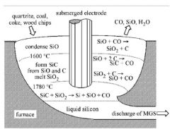
Vacuum arc remelting. SiO in, Si out by C reduction. Still very impure, produces Metal grade silicon (MGS) |
|
|
Describe the Siemens process and resulting Si |
Stage 1 - react Si with HCL - forms SiHCl3. Stage 2 - Fractional distillation - this compoun is exceptionally volatile and can be fairly easily removed Stage 3- reduction back into pure electronic grade Si Conc of impurities reduced to few ppb max, other than C and O |
|
|
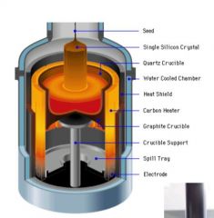
What process for Si crystal growth? Important factors |
Czochralski growth temperature gradient - too shallow and you get constitutional supercooling too step you get convection and non uniform dopant distribution S/L interface speed - must be controlled |
|
|
What is the impurity segragation coefficient and what is it for |
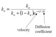
gives effective segragation when equilibrium cannot be established |
|
|
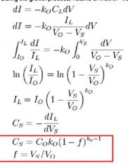
Derive the conc of impurities in a solid product |
|
|
|
What is the result of poorly controlled/ non uniform T gradient? |
Breaks down into cells - impurities segregate to cell boundaries. Non uniform leads to fluctuations in impurity concentration |
|
|
Show how velocity is related to crystal radius. What does this mean? |
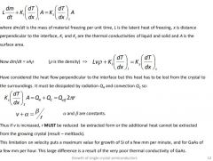
main point: v+B=A/r, so if you increase the velocity you must decrease the radius of the crystal, or melt back will occur |
|
|
Sketch the Czochralski process |
|
|
|
Conc of O in Si. Advantages of O in Slicon |
Most abundant impurity - Keff=1.25 Improves mechanical properties - O hardens the material Gettering - impurities segregate to SiO2 and improve purity |
|
|
disadvantages of O |
Can nucleate dislocations Require surface treatment for removal at top layer where electrical props are otherwise hindered uncontrolled doping effect as a donar |
|
|
What are BMDs and COPS |
Bulk micro defects - provide gettering, removal of harmful transition metals, from the surface COPS crystal originated particles - vacancies diffuse to eachother and cause microvoids, which fill with supersaturated oxygen. Very harmful to electronic gating properties |
|
|
How do TM impurities affect props |
Most are fine - low level transition metals 10^10 in 10^22 Si atoms provide very small minority carrier currents. Only not okay for radiation detectors B is problematic - 10^13 atoms due to Keff 0.8 resulting in max resistivity of 300Ohmm^-1. Not good for high power uses |
|
|
How can we get rid of B in Si growth. Pros and cons |
Float zone growth - melt a portion of the Si and move it up to the top of the Si wafer. Impurities follow the melt up due to their low Keffs. High purity and lifetime, but reduces O so poorer mech props and quite expensive as radius is limited |
|
|
Why is GaAs harder than Si in Czorch |
Volatile - loss of compounds results in non stoichiometry Extended phases fields - always some variation in composition Low yield strenght - always some dislocations Sensitive to stoichiometry - over 48% As is n doped, which is required for high resistivity under is p doped each leading to low resistivities |
|
|
How is good stoichiometry achieved for GaAs Czorch |
Use encapsulation - high pressure argon or boron at the VP of the liquid is used to encapsulate the liquid GaAs, preventing vapourisation. Allows close control of properties |
|
|
Different types of epitaxial growth and the stages? Which stage is arguably most important |
hetero and homo epitaxy, same or different phase. 1)strong bonding to surface bond strength (Ea) 2) diffusion - most important, low activation (Ed) for diffusion gives good surface coverage 3) formation fo clusters (Ec) |
|
|
main type of growth for epitaxial |
Frank Van der Mewre - Ea>Ec, like to bond to surface so diffuse till find a surface atom. Grows in a plane. |
|
|
What is epiitaxial growth called for small lattice difference? Expression for energy and sketch of energies we must consider |
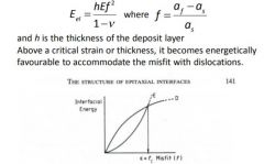
Psuedomorphically. lattice shrinks to fit |
|
|
what kind of structure forms at interface of epitaxia |
dislocations of 60 degree type form on the surface |
|
|
Effects of dislocations on interface properties |
recombination centres - can cause heating, activate more sources and generate more dilocations. Increase resistivity, also normally bad |
|
|
What is CVD? What controls composition and growth rate? normal limiting factors? |
Chemical vapour deposition - vapourize and spray onto the surface. Adsorbed, then thermally decomposes and diffuses away to farm even layer. Comp is controlled by flow rate of the gases, partial pressures, and the rate limiting factors. growth rate on T, and everything above. Limited by supply of substrate or reaction rate on the surface |
|
|
Sketch growth rate of a CVD substrate as a function of flow explaining features |
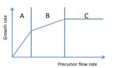
A: fully controlled by flow B: some supersaturation C: complete supersaturation, growth limited by reaction rate |
|
|
T vs growth rate for CVD. explain regions |
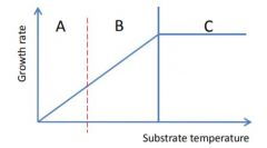
A:Surface reaction kinetics B:surface diffusion C: Transport path limited |
|
|
Where do we use it |
Si - different dopings of Si give very good electrical properties and clean junctions, high resistivities and complex devices Halides Metal oxides |
|
|
Halide VPE fundamentals and main prooblem |
uses PH3 or AsH3 and pure In or Ga which forms GaCl or InCl. Near eq, so comp affect phases produced huge amounts of HCl produced, which disposal N |
|
|
pros and cons of HVPE |
simple and can control phases by flow but can't do Al, or anything that doesn't have a vapour phase, and high Ts lead to impurity inclusions. limited to nm thick |
|
|
Metallo organic CVD differences and pros and cons |
just uses metal alkyls of group 3 which are more readily accessible that put metal vapours, can be done at low T due to instability which mean purer and thinner layers can be grown. But even worse gases produced |
|
|
MBE |
molecular beam deposition - each element is vapourised in separate chambers and flowed in. Huge supersaturations. Low T gives one layer at a time, perfect epitaxy, and limited interdiffusion. Ultra pure |