![]()
![]()
![]()
Use LEFT and RIGHT arrow keys to navigate between flashcards;
Use UP and DOWN arrow keys to flip the card;
H to show hint;
A reads text to speech;
99 Cards in this Set
- Front
- Back
- 3rd side (hint)
|
Printed Circuit Board |
(PCB) -- A conductive series of pathways laminated to a non-conductive substrate that lines the bottom of the computer. |
|
|
|
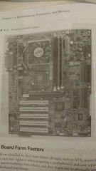
ATX |
(Advanced Technology eXtended) -- A motherboard developed by Intel in the mid 1990s to improve on the classic AT-style motherboard. Processor and memory slots at right angles to expansion cards. Processor runs cooler and you can install full length expansion cards. Standard measure: 12" x 9.6" or 305mm x 244mm |
Primary motherboard in use today. |
|
|
Micro ATX |
(ûATX) -- Designed for enhanced cooling but also to be smaller. With smaller comes less quantity of components. ie, less memory slots, expansion slots, headers, and chassis bays.
Designed with power supplies of lower wattage to keep heat down. Therefore more components like extra USB might require a larger power supply thanks supports.
Measures: 9.6" x 9.6" or 244mm x 244mm |
They are square. |
|
|
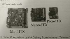
ITX |
Family of form factors designed by VIA as low-power SFFs for specialty uses.
Mini-ITX -- 9.6" x 9.6" Nano-ITX -- 4.7" x 4.7" Pico-ITX -- 3.9" x 2.8" Mobile-ITX -- 2.4" x 2.4" |
|
|
|
Small Form Factor |
SFF |
|
|
|
Form Factor |
Motherboard design classification. |
|
|
|
Bus |
A common collection of signal pathways over which related devices communicate within the computer system. True buses share total bandwidth among all slots. |
|
|
|
SATA |
Serial ATA |
|
|
|
USB |
Universal Serial Bus |
|
|
|
PCIe |
(Peripheral Component Interconnect Express) -- Latest and greatest. Designed to be a replacement for AGP and PCI. It is faster than AGP and yet flexible as PCI. AGP got phased out cause of this.
Serial technology, not parallel.
Seven different link widths are supported: x1, x2, x4, x8, x12, x16, and x32 (x1, x4, and x16 are most common). From 1 to 32 they go thinnest to widest.
Four major versions: 1.x, 2.x, 3.0, and 4.0
Throughput starts at 250MBps per lane per direction for version 1.x and doubled with version 2.x to 500 MBps per lane per direction. |
|
|
|
SCSI |
Small Computer System Interface |
|
|
|
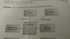
Chipset |
A collection of chips or circuits that perform interface and peripheral functions for the processor.
Usually given a name and model number by the manufacturer. The Northbridge and Southbridge are chipsets. |
|
|
|
Northbridge |
A subset of a motherboard's chipset that performs management of high-speed peripheral communications.
Responsible for communications with integrated video using PCIe and processor-to-memory communications.
Directly connected to the Southbridge. It controls the Southbridge and helps to manage the communications between the Southbridge and the rest of the computer. |
|
|
|
Frontside bus |
(FSB) -- a set of signal pathways connecting the CPU and main memory. |
|
|
|
Backside bus |
(BSB) -- a set of signal pathways between the CPU and Level 2 or Level 3 cache memory. |
|
|
|
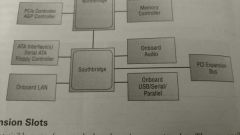
Southbridge |
A subset of the chipset that is responsible for providing support to slower on board peripherals.
Manages communications between peripherals like PS/2, parallel ports, serial and parallel ATA etc. and the rest of the computer. |
|
|
|
Expansion Slots |
Small plastic slots usually from 1 to 6 inches long and about 1/2-inch wide. Used to expand things like video, network, sound and disk interface cards. 3 main types of expansion slots: PCI, PCIe, PCI-X |
|
|
|
PCI |
(Peripheral Component Interconnect) -- About 3 inches long, usually white [not always]. Became popular when Pentium-class processors were a thing. Mostly people have shifted away to PCIe now. Operate at 33MHz or 66MHz over a 32 bit channel. Data rates are 133MBps (most common) and 266MBps. Shared-bus topology used. Slots and adapters are made in 3.3V and 5V versions. |
|
|
|
PCI-X |
(PCI-Extended) -- looks like 64 bit PCI. From 66MHz to 533MHz. 64 bit bus. 4266 MBps throughput. PCIe basically made PCI-X obsolete. Uses shared-bus topology. All adapters run at frequency of slowest inserted adapter. |
|
|
|
Lanes |
The switched point-to-point signal paths between any two PCIe components. Negotiation is used to find the highest mutually supported lanes. |
|
|
|
Link |
The lanes or lane that a switch interconnects between devices. |
|
|
|
AGP |
(Accelerated Graphics Port) -- phased out by PCIe |
|
|
|
Up-plugging |
The ability to use a higher capability slot for a lesser adapter. (You can use a smaller card in a longer slot) If up-plugging is not supported by the motherboard, the smaller card will only run at x1 in the longer slot. Down-plugging (putting a longer card into a smaller slot) is not as commonly possible. |
|
|
|
SLI |
Scalable Link Interface. Done by NVIDIA. |
|
|
|
GPU |
Graphics Processing Unit |
|
|
|
DIMM |
(Dual Inline Memory Module) - circuit boards used for 64-bit RAM. DIMMs differ in number of pins they use. Common configurations are 164-pin, 184-pin, and 240-pin.
DIMM slots are classically black but they've been into color coding for them recently. |
|
|
|
SODIMM |
(Small Outline DIMM) -- a small form factor of memory modules that are used in laptops. |
|
|
|
MicroDIMM |
A small form factor of memory modules that are used in laptops. |
|
|
|
Swap file |
Another word for paging file. Additional space on the hard drive used for storing temporary data for RAM to increase its capacity. The technology that runs this process is referred to as virtual memory.
Relying too much on virtual memory can result in the whole system slowing down noticeably. |
|
|
|
Paging file |
Another word for swap file. Additional space on the hard drive used for storing temporary data for RAM to increase its capacity. The technology that runs this process is referred to as virtual memory. Relying too much on virtual memory can result in the whole system slowing down noticeably. |
|
|
|
PAGEFILE.SYS |
The swap file used in modern Microsoft OS. |
|
|
|
Virtual Memory |
Memory that is used by the RAM but is stored in a swap file on the hard drive. Virtual memory cannot be used directly by the hard drive, it has to be ported over to the RAM to be used. The hard drive can only hold it for later use. Relying too much on virtual memory can make the whole system slowing down. |
|
|
|
Cache Memory |
Very fast form of memory forged from static RAM that is placed between the CPU and the RAM to enhance the speed of the RAM. Cache memory is fast because it predicts what the CPU will need next and it prefetches the data so it's ready when asked. It is known by 3 classifications: L1 Cache, L2 Cache, and L3 Cache. L1 Cache is internal cache that is built into the CPU core. L2 Cache is external cache that is not built into the core and is either in the processor packaging or built into the mother board. If L2 Cache is present in the packaging AND on the mother board, the cache that is built into the motherboard is referred to as L3 Cache. As per distance to move the data, L1 Cache is fastest, L3 Cache is slowest. |
|
|
|
Die |
The processors silicon wafer. Also referred to as the core. |
|
|
|
Core |
The processors silicon wafer. Also referred to as the die. |
|
|
|
L1 Cache |
Level 1 Cache memory. Internal Cache memory. Fastest of the cache memorys. |
|
|
|
L2 Cache |
Level 2 Cache memory. External cache memory that is either in the processor packaging or on the motherboard. It is slower than L1 cache memory, but faster than L3 cache memory if present. |
|
|
|
L3 Cache memory |
Level 3 Cache memory. Cache memory that is built into the mother board while additional cache memory exists that is built into the processor packaging but is not on-die. It is the slowest of the 3 Cache memory types. |
|
|
|
PGA |
(Pin Grid Array) -- a CPU socket type with holes for CPU pins. It's older tech and CPUs that use this array tend to wear out faster than other CPUs. |
|
|
|
LGA |
(Land Grid Array) -- a CPU socket that has spring loaded pins that connect with a grid or lands on the CPU. It's a newer technology and generally it lasts longer than PGA sockets. |
|
|
|
ZIF |
(Zero Insertion Force) -- modern CPU sockets that reduce the need to apply considerable force to the CPU during installation. |
|
|
|
Firmware |
Any software that is encoded in hardware, usually a read-only memory (ROM) chip. |
|
|
|
BIOS |
Basic Input/Output System |
|
|
|
UEFI |
(Unified Extensible Firmware Interface) -- successor to the BIOS. |
|
|
|
TPM |
(Trusted Platform Module) -- security coprocessor that can aid in authenticating boot devices. |
|
|
|
POST |
(Power On Self Test) -- a series of system checks run by the BIOS while booting up. |
|
|
|
MBR |
(Master Boot Record) -- master record used by the BIOS to boot the device after POST finishes it's work. |
|
|
|
CMOS |
(Complementary Metal Oxide Semiconductor) -- a special memory chip that stores info that must be kept to maintain proper computer function [ie date, time, security info, etc.] |
|
|
|
DIP |
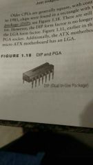
Dual In-line Package |
|
|
|
AMD |
Advanced Micro Devices |
|
|
|
HTT |
(Hyper-Threading Technology) -- an Intel technology that is a form of SMT. |
|
|
|
SMT |
(Simultaneous MultiThreading) -- allows multiple instructions to run in parallel in a processor. |
|
|
|
SMP |
(Symmetric MultiProcessing) -- must be supported by the OS to support HTT. |
|
|
|
Multicore Architecture |
A processor architecture in which multiple, separate dies are in the same package. |
|
|
|
CPU Throttling |
Reducing the operating frequency of the CPU during times of less demand. Used a lot for mobile devices. An automatic operation that is used to protect devices from damage due to high stress. |
|
|
|
APU |
Accelerated Processing Unit |
|
|
|
NX bit |
(No-eXecute bit) -- also known as the disable execute bit is a bit that can denote an area of memory as off limits for execution. It helps protect against buffer overrun attacks. Intel refers to the NX bit as the eXecute Disable (XD) bit. |
|
|
|
DEP |
(Data Execution Prevention) -- the Windows XP OS NX support system. |
|
|
|
Buffer |
A temporary storage area that takes some of the load off of the primary circuit. Interchangeable with register since the temporary storage is in a register. |
|
|
|
ECC |
(Error Correcting Code) -- memory error detection that runs check bits through an algorithm that SHOULD produce all 0s at the end. If only 1 error exists in an 8 bit set, the error can be corrected. |
|
|
|
Parity Checking |
Rudimentary checking scheme that offers no error correction. The 4 main types are... 1. Even 2. Odd 3. Mark 4. Space Even and odd are used in systems that actually compute parity. Mark and space are used in systems that don't compute parity but expect a fixed value in the parity location. |
|
|
|
Memory Bank |
A set of 9 memory chips, 8 of which are used for actual memory while 1 is used to support parity. For the 8 other chips. |
|
|
|
DRAM |
(Dynamic Random Access Memory) -- needs a constant refresh signal or memory will be lost. Used for memory expansion cause it's cheaper. |
|
|
|
ADRAM |
(Asynchronous DRAM) -- slow because of the need for using wait states for fast CPUs. Not used anymore. |
|
|
|
FPM DRAM |
(Fast Page Mode DRAM) -- not used anymore. |
|
|
|
EDO DRAM |
(Extended Data Out DRAM) -- not used anymore. |
|
|
|
BEDO DRAM |
(Burst Extended Data Out DRAM) -- not used anymore. |
|
|
|
SDRAM |
Synchronous DRAM |
|
|
|
SDR SDRAM |
(Single Data Rate Synchronous DRAM) -- original Synchronous DRAM. Now considered a legacy RAM tech. Ever clock tick would push 1 bit of data per pin. Memory modules were PC66, PC100, and PC133 (named off of the clock rate of FSB) |
|
|
|
DDR SDRAM |
(Double Data Rate Synchronous DRAM) -- double pumps data by transferring 2 bits of data for every clock tick; 1 for the rising edge, 1 for the falling edge. |
|
|
|
DDR2 SDRAM |
(Double Data Rate, Version 2 Synchronous DRAM) -- still double pumps data, but also splits the FSB clock rate in 2 internally so that 4 bits of data are pushed through every FSB clock tick; 1 for both rising edges, and 1 for both falling edges. Also, peak voltage is lowered to 1.8V instead of 2.5V to keep down power consumption. |
|
|
|
DDR3 SDRAM |
(Double Data Rate, Version 3 Synchronous DRAM) -- a memory module that further doubles the amount of data pushed through from DDR2 SDRAM. Then peak voltage is again lowered to 1.5V from the 1.8V of DDR2 SDRAM |
|
|
|
SRAM |
(Static Random Access Memory) -- RAM that doesn't require a refresh signal. More expensive, but much faster than DRAM. Typically only used for cache memory. |
|
|
|
ROM |
Read Only Memory |
|
|
|
PROM |
Programmable Read Only Memory |
|
|
|
EPROM |
(Eraseable Programmable Read Only Memory) -- Erases by flashing it with ultraviolet light. |
|
|
|
QPI |
QuickPath Interconnect. |
|
|
|
QPI |
QuickPath Interconnect. |
|
|
|
SIMM |
Single Inline Memory Module |
|
|
|
SIPP |
Single Inline Pin Package |
|
|
|
144-pin |
SODIMM -- SDR SDRAM |
|
|
|
200-pin |
SODIMM -- DDR/DDR2 SDRAM |
|
|
|
204-pin |
SODIMM -- DDR3 SDRAM |
|
|
|
72-pin |
SIMM or old 32 bit SODIMM configuration. |
|
|
|
168-pin |
DIMM -- SDR SDRAM |
|
|
|
184-pin |
DIMM -- DDR SDRAM |
|
|
|
240-pin |
DIMM -- DDR2/DDR3 SDRAM |
|
|
|
100-pin |
Old 32 bit SODIMM configuration. |
|
|
|
LGA 775 (Socket T) |
Intel -- Pentium 4 Pentium 4 Extreme Edition Pentium D Celeron D Pentium Extreme Edition (dual core) Core 2 Duo Core 2 Extreme Core 2 Quad Xeon Celeron (4xx, Exxxx series) |
|
|
|
LGA 1156 (Socket H) |
Intel -- Celeron (G1xxx series) Core i3 Core i5 Core i7 (8xx series) Pentium (G6xxx series) Xeon (34xx series) |
|
|
|
LGA 1155 (Socket H2) |
Intel -- Replacement for LGA 1156 Celeron (G4xx and G5xx) Ivy Bridge |
|
|
|
LGA 1150 (Socket H3) |
Intel -- Replacement for LGA 1155 to support Haswell and Broadwell processors |
|
|
|
LGA 1366 (Socket B) |
Intel -- Core i7 (9xx series) Xeon (35xx, 36xx, 55xx, 56xx series) Intel Celeron P1053 |
|
|
|
LGA 2011 (Socket R) |
Intel -- Replacement for LGA 1366 Has 3 versions that are not electrically compatible with each other. LGA 2011-0 Sandy Bridge-E (Core i7-38xx and i7-39xx) Sandy Bridge-EP (Xeon E5) Ivy Bridge-E (Core i7-48xx and i7-49xx) Ivy Bridge-EP (Xeon E5 v2) LGA 2011-1 Ivy Bridge-EX (Xeon E7 v2) LGA 2011-v3 Haswell-E (x99 chipset) Haswell-EP (Xeon E5 v3) Supports DDR4 memory |
|
|
|
Socket AM3 |
AMD -- DDR3 memory support only Phenom II Athlon II Sempron Opteron 138x Some AM3+ CPUs |
|
|
|
Socket AM3+ |
AMD -- specified for CPUs with Bulldozer microarchitecture Can accept AM3 CPUs |
|
|
|
Socket FM1 |
AMD -- AMD Fusion APUs (Early A series) |
|
|
|
Socket FM2 |
AMD -- a 904-pin socket for Trinity and Richland APUs. |
|
|
|
Socket FM2+ |
AMD -- 906-pin socket for Steamroller APUs Kaveri Godavari Accepts FM2 CPUs as well. |
|