![]()
![]()
![]()
Use LEFT and RIGHT arrow keys to navigate between flashcards;
Use UP and DOWN arrow keys to flip the card;
H to show hint;
A reads text to speech;
83 Cards in this Set
- Front
- Back
|
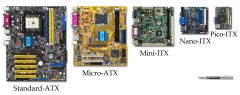
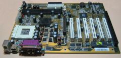
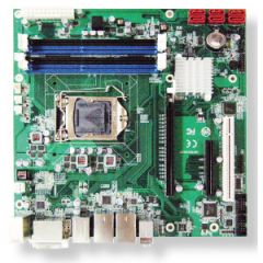
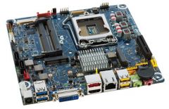
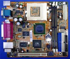
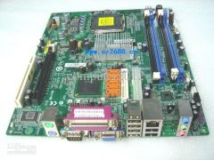
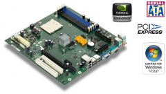
Motherboard Form Factors |
|
|
|
ATX form factor |
|
|
|
MicroATX form factor |
|
|
|
Mini-ITX (a.k.a. ITX) form factor |
|
|
|
FlexATX form factor |
|
|
|
BTX form factor |
|
|
|
MicroBTX form factor |
|
|
|
PicoBTX form factor |
|
|
|
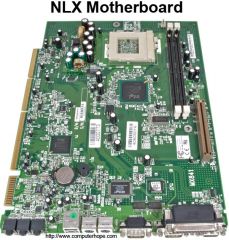
NLX form factor |
|
|
|
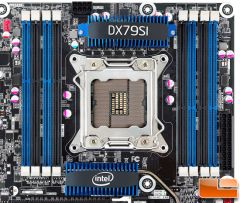
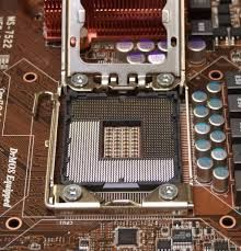
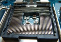
Sockets For Intel Processors |
|
|
|
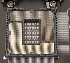
LGA2011 Intel Socket |
Used by Processor Family: Second Generation (Sandy Bridge) Core i7 Extreme, Core i7, Core i5, Core i3, Pentium, and Celeron Description:
|
|
|
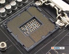
LGA1155 and FCLGA1155 Intel Sockets |
Used by Family Processor: Third Generation (Ivy Bridge) Core i7, Core i5 Second Generation (Sandy Bridge) Core i7 Extreme, Core i7, Core i5, Core i3, Pentium, and Celeron Description:
|
|
|
LGA1156 or Socket H or H1 |
Used by Processor Family: Core i7, Core i5, Core i3, Pentium, and Celeron Description:
|
|
|
LGA1366 or Socket B |
Used by Processor Family: Core i7, Core i7 Extreme Description:
|
|
|
LGA771 or Socket J |
Used by Processor Family: Core 2 Extreme Description:
|
|
|
LGA775 or Socket T |
Used by Processor Family: Core 2 Extreme, Core 2 Quad, Core 2 Duo, Pentium Dual-Core, Pentium Extreme Edition, Pentium D, Pentium Pentium 4, and Celeron Description:
|
|
|
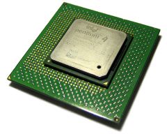
Socket 478 |
Used by Processor Family: Pentium 4, Celeron Description:
|
|
|
Socket 423 |
Used by Processor Family: Pentium 4 Description:
|
|
|
Sockets and processors use different methods to make the contacts between them. What is the list of methods? |
|
|
|
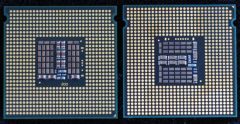
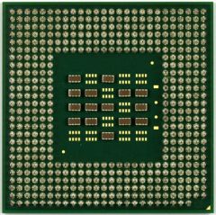
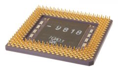
pin grid array (PGA) |
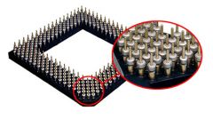
This socket method uses holes aligned in uniform rows around the socket to receive the pins on the bottom of the processor. This method in longer used in computers because the small delicate pins on the processor were easily bent as the processor was installed in the socket. But it is use in Intel mobile processors. |
|
|
land grid array (LGA) |
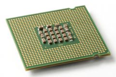
This method socket has blunt protruding pins on the socket that connect with lands or pads on the bottom of the processor. This method generally give better contracts than PGA sockets, and the processor doesn't have the delicate pins so easily damaged during an installation. The first LGA was LGA 775. |
|
|
flip-chip land grid array (FCLGA) and flip-chip pin grid array (FCPGA) |
The flip-chip method is a chip that flips over so that the top of the chip is on the bottom and makes contact with the socket. LGA1155 and FCLGA1155 sockets are not compatible. |
|
|
staggered pin grid array (SPGA) |
The method in which a socket has pins staggered over the socket to squeeze more pins into a small space. |
|
|
ball grid array (BGA) |
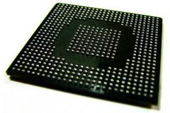
Is a connection that is not really a socket. ?? The processor is soldered to the motherboard, and the two are always purchased as a unit. |
|
|
zero insertion force (ZIF) sockets |
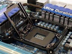
are current sockets that have 1 or 2 levers on the sides of the socket. These levers help applied forces when inserting the processor into the socket. |
|
|
Sockets for AMD Processors |
AMD choices to use the PGA socket architecture for its desktop processors. AMD sockets:
|
|
|
FM2 |
.. |
|
|
FM1 |
... |
|
|
AM3+ |
... |
|
|
AM3 or AMD3 |
... |
|
|
AM2+ or AMD2+ |
... |
|
|
Socket F (1207) or F |
... |
|
|
AM2, AMD2, or M2 |
... |
|
|
Socket 940 |
... |
|
|
Socket 939 |
... |
|
|
Socket 754 |
... |
|
|
Socket A |
... |
|
|
The Chipset |
is a set of chips on the motherboard that works closely with the processor to collectively control the memory, buses on the motherboard, and some peripherals. The chipset must be compatible with the processor it serves. Major Chipset Manufacturers:
|
|
|
Intel Chipsets |
Intel has produced far too many chipsets to list them. The list of the more significant chipset families by Intel:
|
|
|
Intel: North Bridge and South Bridge use a hub architecture. |
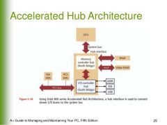
Beginning with the release in 2006 of the Intel i800 series of chipsets, a hub using the Accelerated Hub Architecture is used to connect buses. |
|
|
Accelerated Hub Architecture |
This hub has a fast and slow end, and each end is a separate chip on the motherboard. The two chips are North Bridge (the fast end of the hub) and South Bridge (the slower end of the hub) |
|
|
North Bridge |
A chipset use in the Accelerated Hub Architecture that connects faster I/O buses (for example, the video bus) to the system bus. It contains the graphics and memory controller, and connects directly to the processor by a 64-bit bus, called the Front Side Bus (FSB), systembus, or host bus. |
|
|
South Bridge |
A chipset that is used in Accelerated Hub Architecture. This hub connects slower I/O buses (for example, a PCI bus) to the system bus. It contains the I/O controller hub (ICH). All I/O (input/output) devices, except video, connect to the hub by using the slower South Bridge. |
|
|
Intel: X58 chipset architecture with memory controller in the processor. |
The release of the X58 chipset in 2008 the memory controller was contained in the processor housing. The memory connects directly to the processor rather than to the North Bridge. Some board comes with a clipped heat sink to keep the North Bridge chipset cool. Another significant change is the 64-bit Front Side Bus was replaced with a technology called the QuickPath Interconnect (QPI). |
|
|
QuickPath Interconnect (QPI) |
The technology used first by the Intel X58 chipset for communication between the chipset and the processor using 16 serial lanes similar used by PCI Express. It replaced the 64-bit wide Front Side Bus from previous chipsets. |
|
|
Intel: Nehalem chipsets |
Nehalem chipsets work as X58 chipset architecture. X58 chipset is part of the Nehalem chipsets family. Nehalem chipsets is know as Intel's previous generation chipsets. It support the Intel LGA1366 socket, the Core i7 processors, and PCI Version 2. They can also support either SLI or CrossFire technologies. (SLI and CrossFire are two competing technologies that allow for multiple video cards installed in one system.) |
|
|
Intel: Sandy Bridge chipsets with the memory and graphics controller in the processor. |
In 2011, Intel introduced its second-generation chipsets and sockets, which it code-named Sandy Bridge technologies. Rather than using the traditional North Bridge and South Bridge, only one chipset housing is needed, which houses the Platform Controller. The processor interfaces directly with PCI Express 2.0 bus as well as with memory to obtain faster graphics. Therefore, both memory controller and graphics controller are contained with all Sandy Bridge processors. |
|
|
Intel: Ivy Bridge chipsets |
Third-generation processors and chipsets by Intel, released in 2012 and codenamed Ivy Bridge, use less power, squeeze more transistors into a smaller space, and perform better than earlier products. It uses a single Platform Controller Hub. |
|
|
AMD chipsets |
AMD purchased ATI Technologies, a maker of chipsets and graphics processors (called a graphics processor unit or GPU), in 2006, which increase AMD chipset and GPU offerings. |
|
|
Significant chipsets by AMD include the following: |
|
|
|
NVIDIA, SIS, and VIA chipsets |
All make graphics processors and chipsets for both AMD and Intel processors. Recall that NVIDIA's method of connecting multiple video cards in the same system is called SLI. If you're planning a gaming computer with two video cards, check out a motherboard that supports SLI and uses the nForce chipset. In motherboard ads, look for the SLI and nForce logos. |
|
|
Buses and Expansion Slots |
When you look carefully at a motherboard, you see many fine lines on both the top and the bottom of the board's surface. These lines, sometimes called traces, are circuits or paths that enable data, instructions, and power to move from component to component on the board. |
|
|
Bus |
is the system pathways used for communication, protocol, and methods. ( A protocol is a set of rules and standards of two entities. Protocols are use for communication.) The parts of the bus that we are most familiar with are the lines of the bus that are used for data; these lines are called the data bus. |
|
|
More info of Buses |
A bus can also carry electrical power (to power components on the motherboard), control signals (to coordinate activity), and memory addresses (to instruct one program toward another program where to find data or instructions). |
|
|
Data on buses |
All data and instructions inside a computer exist in binary, which means there are only two states: on and off. Binary data is put on a line of a bus by placing voltage on that line. The CPU or other devices interpret the voltage, or lack of voltage, on each line on the bus as binary digits (0s and 1s). |
|
|
data path size |
is the width of a data bus. Some buses have data paths that are 8, 16, 32, 64, 128, or more bits wide. For example, a bus that transmit data with eight wires or eight lines is called an 8-bit bus. An 8-bit data bus between the CPU and memory that transmit the letter A (binary 0100 001) are placed on the lines at the same time: no voltage for binary zero and voltage for binary one. For every eight bits of a bus, a bus might use a ninth bit for error checking. Adding a check bit for each byte allows the component reading the data to verify that it is the same data written to the bus. |
|
|
system clock (system timer) |
Is an interesting lines, or circuits, on a bus that dedicates in timing the activities on the motherboard much like a metronome helps a musician with timing. Its the chipset that sends out a continuous pulsating electrical signal on one line of the system bus. This one system clock line, dedicated in carrying the pulse, is read by other components on the motherboard (including the processor, bus slots, memory slots, and so forth) and ensures that all activities are synchronized. Each device works on a clock cycle or beat of the clock. If the processor requests something from a slow device and the device is not ready, the device issues a wait state, which is a command to the processor to wait for slower devices to catch up. |
|
|
The speed of memory, Front Side Bus, processor, or other component is measured in ... |
hertz (Hz), which is one cycle per second; megahertz (MHz), which is one million cycles per second; and gigahertz (GHz), which is one billion cycles per second. It the measure of continuous flow or the clock speed that the device can reach.
|
|
|
Info about implying terms of speed |
When referring to the speed of the CPU and memory, frequency is more accurate to describe the devices because the term "speed" implies a continuous flow, while the term "frequency" implies a digital or binary flow: on and off, on and off. Meaning the speed when the voltage turn on and off. |
|
|
Different Buses Info |
A motherboard can have more than one bus, each using a different protocol, speed, data, path size, and so on. Throughput is sometimes called bandwidth. Throughput is the amount of material or items passing through a system or process. |
|
|
expansion bus, local bus, and local I/O bus |
Buses can variety from expansion bus, local bus, local I/O bus, or local video bus. A bus that does not run in sync with the system clock is called an expansion bus.
Most buses today are local buses, meaning they run in sync with system clock. If a local bus connects to the slower I/O controller hub or South Bridge of the chipset, it is called a local I/O bus. |
|
|
video bus
|
Video card needs to run at a faster rate than other adapter cards, which is why one slot always connects to the faster end of the chipset, the North Bridge, or directly to the processor when using Sandy Bridge or Ivy Bridge technology. Older boars used AGP video slots, and today's boards use PCI Express x16 slots for video. These video buses that connect to the North Bridge or to the processor are called local video buses. |
|
|
The List of Various Buses |
|
|
|
PCI Express Version 2
|
Data Path in Bits: Serial with up to 32 lanes Address Lines: Up to 32 lanes Bus Frequency: 2.5 GHz Throughput: Up to 500 MB/sex per lane in each direction |
|
|
PCI Express Version 1.1
|
Bus Type: Local video and local I/O
Data Path in Bits: Address Lines: Bus Frequency: 1.25 GHz Throughput: |
|
|
PCI Express Version 1
|
Bus Type: Local video and local I/O
Data Path in Bits: Address Lines: Bus Frequency: 1.25 GHz Throughput: |
|
|
PCI-X |
Bus Type: Local I/O Data Path in Bits: Address Lines: Bus Frequency: 66, 133, 266, or 533 MHz Throughput: |
|
|
PCI |
Bus Type: Local I/O Data Path in Bits: Address Lines: Bus Frequency: 33, 66 MHz Throughput: |
|
|
AGP 1x, 2x, 3x, 4x, 8x |
Bus Type: Local video Data Path in Bits: Address Lines: Bus Frequency: 66, 75, 100 MHz Throughput: |
|
|
FireWire 400 and 800 |
Bus Type: Local I/O or expansion Data Path in Bits: Address Lines: Bus Frequency: NA Throughput: |
|
|
USB 1.1, 2.0, and 3.0 |
Bus Type: Expansion Data Path in Bits: Address Lines: Bus Frequency: 3 MHz Throughput: |
|
|
Conventional PCI
|
PCI Version 2.x introduce the 64-it, 3,3 V PCI slot, doubling data throughput of the bus. These slots are usually white. Because a card can be damaged if installed in the wrong voltage slot, a notch in a PCI slot distinguishes between a 5V slot and a 3.3 V slot. |
|
|
PCI-X
|
The next evolution of PCI is PCI-X, which uses a 64-bit path and had 3 major revisions; the last and final revision is PCI-X 3.0 |
|
|
PCI Express (PCIe)
|
uses an altogether different architectural design than conventional PCI and PCI-X; PCIe is not backward compatible with either. The existence is continuing
|
|
|
PCI Riser Cards Used to Extend the Slots
|
...
|
|
|
AGP Buses
|
... (no need to study that. That technology is old) |
|
|
On-Board Ports and Connectors
|
Ports coming directly off the motherboard are called on-board ports or intergraded components. When you purchase a motherboard, the package include an I/O shield, which is the plate that you install in the computer case that provides holes for these I/O ports. The I/O shield is the size designed for the case's form factor. |
|
|
header
|
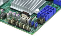
If a connector is a group of pins sticking up on the board, the connector is called a header. |
|
|
system panel connectors
|
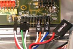
controls a computer power button, reset button, and LED's. They need to be connect to show
CPU small light bulbs and turn on the computer. |
|
|
Configuring a Motherboard
|
Before technicians need to open the case to configure the motherboard. But today's convenient method is to store configuration data in CMOS RAM.
|
|
|
CMOS (complementary metal-oxide semiconductor) and CMOS RAM
|
A program in BIOS, called BIOS setup or CMOS setup, can easily make changes to the settings stored in CMOS RAM. |
|
|
Find the Motherboard Documentation
|
Click Start, type msinfor32.exe in the Search box, and press Enter. In the System Information window, click System Summary. In the System Summary information in the right pane, look for the motherboard information labeled as the System Manufacturer and System Model.
|
|
|
Using Jumpers to Configure a Motherboard
|
A jumper is two small ports or metal pins that stick up off the motherboard that is open or closed. Jumpers can be set to clear both passwords. A jumper can be set to undo the update. |